A scion of a Cretan family, Mr. Hatzakis worked since 1961 in the research laboratories of IBM and from 1989 until retirement in the National Centre for Scientific Research Demokritos in Athens. In all these years he was an inventor in more than 20 patents, and an author in hundreds of publications. He was a member of the American Academy of Engineering, IBM fellow, and a member of many professional organizations such as the IEEE.
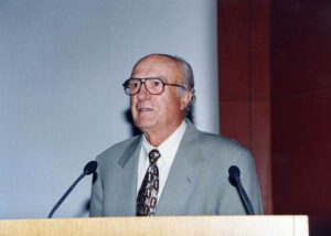
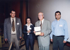
As he stated during the award ceremony before more than 600 delegates at the international conference Micro and Nano Engineering in 2006 in Barcelona, Spain, but also at other similar awards in Demokritos research center and elsewhere, “I was fortunate to live in a productive era full of discoveries, and I had the pleasure of being part of the amazing progress of micro and nano electronics“.
He and his colleagues were the first to propose the use of electrons instead of light to reduce the dimensions of circuits by constructing the first electron beam lithography system (“Electron-Beam Lithography draws a finer line” T.H.P. Chang, M. Hatzakis, A.D. Wilson, A. N. Broers, Electronics 1977)
Simplicity and genius are not divided. Indeed, searching for suitable materials to respond to electrons, they thought to grind a common plastic “plexiglass” (PMMA), dissolve it into a solvent and then coat it on a silicon wafer. PMMA became the first electron bean resist, and PMMA has remained to this day (50 years later) the material with the best resolution. (“High-resolution Positive Resists for Electron-beam Exposure” I. Haller, M. Hatzakis, R. Srinivasan IΒM, Journal of research and development, vol. 12(3), (1968) 251-256)
They were also the first to discover a metallization process that almost everyone uses today, known with the name “the lift-off process“. These two processes went into production for mask and circuit manufacturing at IBM. At the time when electronic circuits had a minimum dimension of 10000 nanometers (10 micrometers) Mr. Hatzakis’ team built had already built a transistor of 500 nanometers, and 100nm structures. (“Electron Resists for Microcircuit and Mask Production” M. Hatzakis Journal of the Electrochemical Society, vol. 116-7, (1969) 1033-1037)
(“Microcircuits by Electron Beam” A. N. Broers, M. Hatzakis Scientific American, vol. 227-5, (1972) 34-44). Therefore, as early as 1972, Mr. Hatzakis’ team was a pioneer in nanotechnology.
During the 80s his team has built even smaller 30nm structures (“Direct electron-beam patterning for nanolithography” K.L. Lee, M. Hatzakis Journal of Vacuum Science and Technology B, vol. 7(6), (1989) 1941-1946). Mr. Hatzakis’ activity continued intensively in Greece where the entire IBM team contributed to the installation of an electron beam lithography system. (“An advanced epoxy novolac resist for fast high-resolution electron-beam lithography” P. Argitis, I. Raptis, C.J. Aidinis, N. Glezos, M. Baciocchi, J. Everett, M. Hatzakis Journal of Vacuum Science and Technology B, vol. 13-6, (1995) 3030-3034).
During his tenure as director, the Institute of Microelectronics of NCSR Demokritos grew, gained international prestige, and established itself in the international field of micro and nanotechnology and electronics. In 1997 the MNE (Micro and Nano Engineering) conference was held in Greece bringing international scientists (such as Heini Rohrer Nobel Laureate for STM, AFM see H. Rohrer “Nanoengineering Beyond Nanoelectronics”, Microelectronic Engineering 41/42 (1998) 31-36), as well as Industry CEOs including Texas Instruments, Photronics, Motorola, Shipley, Hellenic Investment Center (Microelectronic Engineering 41/42 (1998) 1-71). The MNE conference came in Greece also in 2008 in Athens, where Mike was very active, and 2019 (www.mne2019.org).
But beyond science the ethos and the quality of man dominate, Mr. Hatzakis excelled in both of them. He treated young researchers like a father, while when addressing politicians, researchers and academics he tried to emphasize the need to attract investment in the field of Microelectronics, in Greece and in Europe, to create a local industry that together with research institutes and universities will lead to the creation of a healthy ecosystem around semiconductor technology.
In a sense, Michael Hatzakis was the ancestor of today’s initiative of Europe and America entitled Chips Act. He will remain a shining example engraved in our memory for being humble, and simple, and for his philosophical approach to life that helped him overcome difficulties.
Michael Hatzakis and IBM and NCSR Demokritos Research Director